The spectrograph is shown in detail in Fig. 2. It is composed of commercially available components including a hemispherical analyser, a 4-element focusing lens and a two-dimensional position sensitive detector (2D-PSD). Both analyser and lens were made of aluminum with their inner surfaces coated by soot to reduce secondary electron emission and diminish the effects of contact potentials. An additional shield placed around the outer hemisphere was found to be necessary, substantially reducing background electron counts. The 2D-PSD consists of a pair of 40 mm active area multichannel plates (MCP) and a resistive anode encoder (RAE). The entire detection system was mounted in its own cylindrical base and further shielded from background electrons.
The analyser consists of two hemispherical shells with outer ( ![]() )
and inner (
)
and inner ( ![]() ) radii of 130.8 mm (5.15
) radii of 130.8 mm (5.15 ![]() ) and 72.4 mm (2.85
) and 72.4 mm (2.85 ![]() ),
respectively.
The two shells are supported on a cylindrical base plate
from which they are electrically isolated. The base plate constitutes the
relative ground of the analyser and can be independently biased with
a plate voltage
),
respectively.
The two shells are supported on a cylindrical base plate
from which they are electrically isolated. The base plate constitutes the
relative ground of the analyser and can be independently biased with
a plate voltage ![]() when deceleration of electrons prior to analysis is
required.
The four-element lens is also supported from this plate
with the exit lens element and base plate being on the same potential
when deceleration of electrons prior to analysis is
required.
The four-element lens is also supported from this plate
with the exit lens element and base plate being on the same potential ![]() .
At present, 4 mm apertures are used at the entrance and exit of the lens.
On the upper part of the analyser there is a
circular opening where the detector is mounted.
A 90% transmission grid is placed at this opening for better termination
of the electric field.
The two hemispheres with the common base plate are mounted on a
second plate which constitutes
the absolute ground of the spectrograph. Sapphire balls
are used for electrical isolation of the various components of
the spectrograph.
.
At present, 4 mm apertures are used at the entrance and exit of the lens.
On the upper part of the analyser there is a
circular opening where the detector is mounted.
A 90% transmission grid is placed at this opening for better termination
of the electric field.
The two hemispheres with the common base plate are mounted on a
second plate which constitutes
the absolute ground of the spectrograph. Sapphire balls
are used for electrical isolation of the various components of
the spectrograph.
The properties of hemispherical analysers and their
operation have been extensively
described in the literature for slit spectrometer (see for example
the recent review by Roy and Tremblay [1] and references therein)
and to a lesser extent for spectrographs
[2, 3, 4, 5, 6]
(i.e. exit slit replaced by PSD).
Our hemispherical
analyser has its entrance aperture centered
at a radial distance ![]() =82.6 mm (3.25
=82.6 mm (3.25 ![]() ).
This makes it atypical since most analysers have
).
This makes it atypical since most analysers have ![]() at or near the mean radius
at or near the mean radius ![]() (=101.6 mm or 4
(=101.6 mm or 4 ![]() in our case) and
in our case) and ![]() [7].
[7].
Computer simulations using the ion-optics package SIMION 3D [8]
indicate that this asymmetric
entrance optimizes the focusing properties of the analyser.
When the fractional interradial separation ![]() is large, such as in the
case of spectrographs (here
is large, such as in the
case of spectrographs (here ![]() ),
the effect of the entrance and exit fringing fields
can result in large departures
from the 1/r potential dependence of an ideal spherical condenser.
This leads to the well-known
shifting of the focus point from the exit plane (at
the deflection angle
),
the effect of the entrance and exit fringing fields
can result in large departures
from the 1/r potential dependence of an ideal spherical condenser.
This leads to the well-known
shifting of the focus point from the exit plane (at
the deflection angle ![]() )
to smaller deflection angles (
)
to smaller deflection angles ( ![]() )
with adverse effects on the
energy and time-resolution properties of such an instrument.
Various correction schemes have been proposed [9], the most common
solution (albeit cumbersome) being the use of multiple rings or strips
to terminate the electric field at the ends of the hemispherical electrodes.
[3, 10].
Our SIMION simulations [11, 12]
indicate that for particular
combinations of asymmetric entrance points
)
with adverse effects on the
energy and time-resolution properties of such an instrument.
Various correction schemes have been proposed [9], the most common
solution (albeit cumbersome) being the use of multiple rings or strips
to terminate the electric field at the ends of the hemispherical electrodes.
[3, 10].
Our SIMION simulations [11, 12]
indicate that for particular
combinations of asymmetric entrance points ![]() and non-zero entrance potentials
(
and non-zero entrance potentials
( ![]() ) the focus point can be moved back to the exit plane,
thus avoiding the neccessity of
tedious correction schemes.
A detailed presentation of these results will be presented elsewhere
[13].
) the focus point can be moved back to the exit plane,
thus avoiding the neccessity of
tedious correction schemes.
A detailed presentation of these results will be presented elsewhere
[13].
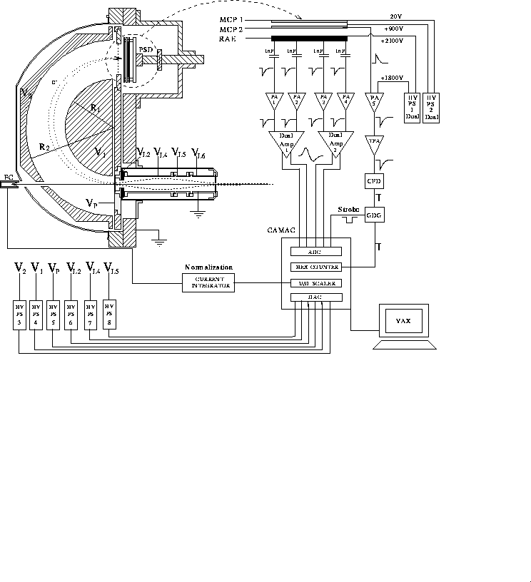
Figure: The electronics diagram
The analyser is run at fixed voltages. Their values for the low resolution (non-decel) mode have been derived for the ideal spherical condenser case and are (in volts) [13]:
with ![]() and
and ![]() the entrance and exit points of the
cental trajectory, i.e. the path of
an electron with
kinetic energy
the entrance and exit points of the
cental trajectory, i.e. the path of
an electron with
kinetic energy ![]() (in eV) entering the analyser normally.
In this configuration, i.e. when
(in eV) entering the analyser normally.
In this configuration, i.e. when ![]() , the central trajectory
defines an elliptical orbit rather than a circle as in the case of symmetric
entrance.
, the central trajectory
defines an elliptical orbit rather than a circle as in the case of symmetric
entrance.
![]() is also known as the tuning energy of the analyser [7].
The voltages
is also known as the tuning energy of the analyser [7].
The voltages ![]() and
and ![]() given by Eq. 1,
were found to be close to the ones actually used (either in the
SIMION simulation or the real analyser). The value of
given by Eq. 1,
were found to be close to the ones actually used (either in the
SIMION simulation or the real analyser). The value of ![]() was found from simulations to give optimal
focusing for values
was found from simulations to give optimal
focusing for values ![]() and were close to the ones
found empirically and used on the real analyser.
and were close to the ones
found empirically and used on the real analyser.
The acceptance energy range of the analyser is close to 20%,
which means that the energy range ![]() can be
recorded simultaneously. Thus, the double focusing properties of the
hemispherical analyser together with the simultaneous recording
of a large energy slice due to the use of a PSD lead to
substantial savings in collection time.
can be
recorded simultaneously. Thus, the double focusing properties of the
hemispherical analyser together with the simultaneous recording
of a large energy slice due to the use of a PSD lead to
substantial savings in collection time.
The four-element focusing lens
provides a virtual slit for the incoming electrons by focusing them at the
entrance of the analyser. The lens can be used to
also decelerate the electrons (high resolution or decel mode)
while focusing them for improved energy resolution.
The entrance lens element ![]() (see Fig. 2)
is always grounded, while the exit lens
element is on potential
(see Fig. 2)
is always grounded, while the exit lens
element is on potential ![]() which is also
grounded when running in the low resolution (non-decel) mode.
To date, we have only utilised three of the four elements, with
experimentally determined values of
which is also
grounded when running in the low resolution (non-decel) mode.
To date, we have only utilised three of the four elements, with
experimentally determined values of
![]() ,
, ![]() and
and ![]() . Further
control of the lens transmission and angular magnification
can be attained by also using lens element L2 and will be pursued in
the near future.
. Further
control of the lens transmission and angular magnification
can be attained by also using lens element L2 and will be pursued in
the near future.
The electrons are detected along a narrow strip
over the PSD surface due to the double
focusing properties of the analyser.
Traditional electronics for 2-D PSD's are used. The
electronics diagram is also shown in
Fig. 2. Signals from the four corners of the RAE are
decoupled by 1nF capacitors, amplified and sent to CAMAC ADCs.
The strobing signal to the ADC comes from the back of the second MCP.
The CAMAC
electronics along with all the power supplies in use are controlled by a
VAX computer. The position spectrum is recorded in a ![]() channels array using
the XSYS data acquisition package.
Monoenergetic electrons from an electron gun were used to energy
calibrate the PSD. The transformation between channels and energy
was found to be linear to a high approximation.
An important restriction in the singles counting rate
in this configuration is the large dead time of the
CAMAC electronics. Thus, counting rates had to be limited to
less than 5kHz to maintain dead time below
10%. We believe this limitation in counting rate can be
improved at least by a factor of 10
by going to a faster data aquisition system
which we hope to implement in the future.
channels array using
the XSYS data acquisition package.
Monoenergetic electrons from an electron gun were used to energy
calibrate the PSD. The transformation between channels and energy
was found to be linear to a high approximation.
An important restriction in the singles counting rate
in this configuration is the large dead time of the
CAMAC electronics. Thus, counting rates had to be limited to
less than 5kHz to maintain dead time below
10%. We believe this limitation in counting rate can be
improved at least by a factor of 10
by going to a faster data aquisition system
which we hope to implement in the future.